
TSMC’s Secret Move with Nvidia’s HBM Chips Could Shake the Tech World – Are You Ready to Profit?
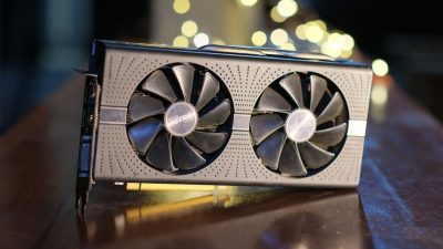
Ever wonder what happens when a tech giant like Nvidia decides it wants its AI memory crafted not just well—but just so, with a single trusted partner handling the rock-solid foundation? Well, buckle up, because Nvidia’s latest move is shaking up the entire memory-making game. Taiwan Semiconductor Manufacturing Company (TSMC) is stepping into the spotlight, armed with its cutting-edge 3nm process technology, ready to build the base dies for Nvidia’s custom high-bandwidth memory stacks, charmingly dubbed NVHBM. Picture this: Samsung, SK Hynix, and Micron—three heavyweights in the memory world—all aligning under TSMC’s umbrella for this project. Now here’s the kicker—Samsung’s jumping into bed with TSMC on HBM base die manufacturing for the very first time. That’s quite the industry plot twist, huh? This isn’t just about tech specs; it’s a bold stroke toward standardizing memory construction, cranking up performance by up to 30% and slashing power consumption by 15%. And Nvidia’s smart—by embedding its own memory controller into the base die, it frees up precious GPU space for other magic. So, the big question is: will this strategic reshuffling rewrite the rules of the AI hardware supply chain, or is it just another chapter in the ongoing game of semiconductor chess? Either way, it’s one heck of a story unfolding right beneath the surface of your favorite gadgets. LEARN MORE
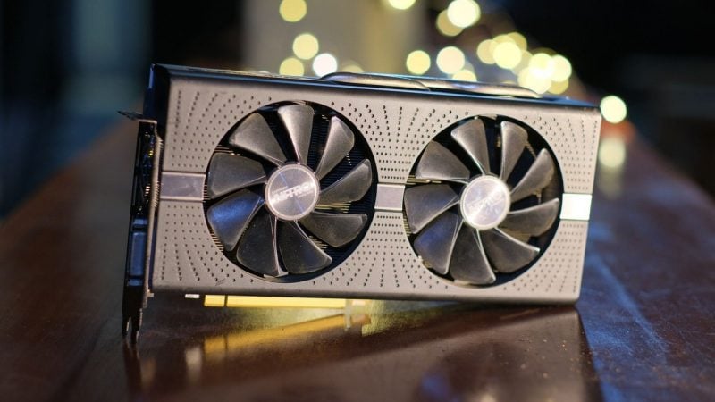
Nvidia wants its AI memory built a very specific way. It also wants one company doing the most important part of the building.
Taiwan Semiconductor Manufacturing Company will reportedly supply its 3nm process technology for the base dies of Nvidia’s custom high-bandwidth memory stacks, a product line Nvidia calls NVHBM. The arrangement, reported on October 18, 2026, draws all three major memory makers into TSMC’s orbit: Samsung Electronics, SK Hynix, and Micron.
The most eye-catching detail involves Samsung. This is reportedly the first time Samsung has worked with TSMC on HBM base die manufacturing specifically.
What Nvidia is actually asking for
Nvidia announced NVHBM in August 2026. The goal was to standardize the way custom HBM gets built, rather than letting each memory supplier take its own approach.
NVHBM moves Nvidia’s own memory controller into the base die. The controller is the logic that directs traffic between the memory and the processor.
Nvidia says the payoff is substantial. NVHBM is designed to deliver up to a 30% increase in memory bandwidth and 15% lower power consumption compared to standard HBM4E.
Pushing the controller into the base die also optimizes area usage on the GPU compute die itself, freeing up space on the processor that Nvidia can put to other uses.
To make this work consistently, Nvidia directed Samsung, SK Hynix, and Micron to use TSMC’s 3nm process for their NVHBM base dies. The aim is standardization, along with a more reliable verification process across all three suppliers.
Three memory makers, three different strategies
Samsung has agreed to use TSMC’s technology for NVHBM. However, it plans to keep some in-house production capacity for standard HBM and other customized memory products.
Micron has confirmed plans to use TSMC’s technology as well. The company is set to outsource both HBM4E and NVHBM base dies to TSMC, and it anticipates volume production by 2027. Micron also expects the shift to bring higher profitability.
SK Hynix previously used TSMC’s 12nm process for earlier HBM4 base dies. Now SK Hynix is prioritizing the 3nm process for future HBM releases, including custom variants.
A quiet reshuffling of the memory business
For years, memory makers handled their own production from top to bottom. The NVHBM arrangement reflects a broader trend in which Samsung, SK Hynix, and Micron are shifting base die production to TSMC.
As AI hardware demands climb, the base die increasingly needs leading-edge logic manufacturing. The result is a growing division of labor: memory companies concentrate on their core DRAM technologies, while foundries take on the advanced logic layers that sit underneath.
What this means for the AI hardware supply chain
For TSMC, the deal deepens an already central position in AI hardware. The company now sits underneath both Nvidia’s processors and, increasingly, the memory stacks that feed them.
For Nvidia, standardizing the base die and embedding its own memory controller lets Nvidia set the rules for how its memory behaves, regardless of which supplier made the DRAM.
There are a few things worth tracking from here. The first is whether Micron hits its anticipated 2027 volume production target for TSMC-made base dies. The second is how much HBM work Samsung ultimately keeps in-house versus routing through TSMC. The third is whether NVHBM delivers on its targets: up to 30% more bandwidth and 15% lower power versus HBM4E are design goals, and real-world shipping products will be the final test.

Fhumsh Wireless Earbuds, Bluetooth 6.0 Headphones HiFi Stereo 50H Playback LED Digital Display Ear Buds with ENC Noise Canceling Headset, IPX7 Waterproof Earphones for Gym/Running/Work(White)
$19.97 (as of October 18, 2026 03:33 GMT +00:00 - More infoProduct prices and availability are accurate as of the date/time indicated and are subject to change. Any price and availability information displayed on [relevant Amazon Site(s), as applicable] at the time of purchase will apply to the purchase of this product.)
Open Ear Wireless Earbuds Bluetooth Headphones, 80H Playtime Stereo Ear Buds with ENC Noise Cancelling, Fast Charging, IPX7 Waterproof Sports Earphones with Earhook for Running/Workouts (Black)
$26.98 (as of October 18, 2026 03:33 GMT +00:00 - More infoProduct prices and availability are accurate as of the date/time indicated and are subject to change. Any price and availability information displayed on [relevant Amazon Site(s), as applicable] at the time of purchase will apply to the purchase of this product.)
Amazon Basics Surge Protector Power Strip, 6-Outlet with 200J Protection, Circuit Breaker, LED Indicator, On/Off Switch, Wall-Mounting, 2ft Extension Cord, White, 2-Pack
$12.59 (as of October 18, 2026 03:22 GMT +00:00 - More infoProduct prices and availability are accurate as of the date/time indicated and are subject to change. Any price and availability information displayed on [relevant Amazon Site(s), as applicable] at the time of purchase will apply to the purchase of this product.)
Medium Hass Avocado
(as of October 18, 2026 03:10 GMT +00:00 - More infoProduct prices and availability are accurate as of the date/time indicated and are subject to change. Any price and availability information displayed on [relevant Amazon Site(s), as applicable] at the time of purchase will apply to the purchase of this product.)












Post Comment